Lab team reports breakthrough in ultrafast, high-resolution nanoscale 3D printing
 (Download Image)
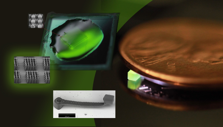
Using a new method of nanofabrication developed at Lawrence Livermore, engineers were able to produce a cuboid structure with nanoscale features that would take several hours with existing two-photon lithography technology in about eight minutes. Researchers also produced the thinnest nanowires ever printed by any similar system — as thin as 140 nanometers in width or about 400 times finer than human hair — and bridge and curved structures that are challenging or even impossible to print at this scale with other techniques.
While 3D printing at the nanoscale — producing intricate features orders of magnitude smaller than the width of a human hair — has significant potential in industry and commercial applications, wide adoption has been impractical because of the slow speed and low throughput of the most widely used nanoprinting technique, two-photon lithography (TPL).
But in the latest issue of Science, posted online today, a team of resesarchers describe a breakthrough in nanoscale 3D printing, developing a scalable method of nanofabrication up to 1,000 times faster than any previous method, without sacrificing resolution, potentially opening the door to cost-effective, large-scale 3D nanoprinting.
“There are always these tradeoffs that engineers need to balance, and that tradeoff also existed in the two-photon lithography process — when engineers build finer features, they lose the rate at which they print. Our work breaks this engineering tradeoff,” said Sourabh Saha, a former LLNL engineer and lead author on the paper. “Second, the throughput boost is such that one can now start using it in real-world applications. A lot of engineers want to use TPL, but they haven’t been able to figure out a way to scale up the process. Our technique solves this problem.”
In the standard serial two-photon lithography process, 3D structures are built by focusing a laser beam to a very fine spot within a photopolymer material. The volumetric pixels, or “voxels,” harden at each point the beam hits, the unpolymerized liquid is removed, and engineers are left with the solid 3D structure. But because the points are so small — less than a micron — it takes a great deal of time to build the structure. With the new method developed at LLNL, called femtosecond projection TPL (FP-TPL), the team parallelized the process by using a broadband, ultrashort-pulsed laser, besting the standard TPL in not only throughput, but also in feature size.
Saha, who recently joined the faculty at Georgia Tech as an assistant professor but performed the work while at LLNL, explained that although other researchers have tried similar parallelization approaches, they’ve resulted in poor resolution and thick features. The LLNL team discovered how to project a million focused points of light at once, while also maintaining light projections thinner than a micron. By temporally focusing the laser and altering the duration of the laser pulse as the light travels through the material, researchers were able to control the intensity of light in the material, creating a gradient of intensity and printing only at high-intensity planes.
Using this parallelized FP-TPL technique, the LLNL engineers produced the thinnest nanowires ever printed by any similar 3D-printing system — as thin as 175 nanometers in height and 140 nanometers in width, about 400 times finer than human hair. The researchers printed test samples to show the scaling of the FP-TPL technique, including “log-pile” structures, suspended nanowires and curved structures that are challenging to print through serial techniques.
They also printed 1-millimeter-long suspended bridge structures with 90-degree overhangs and submicron features, an “impossible” task using any other 3D-printing technique on this fine scale, Saha said, as well as large millimeter-scale cuboid structures to highlight the superior throughput of their technique. A cuboid structure that would take several hours to print with the serial TPL technique was printed in little more than eight minutes with FP-TPL.
Work will be done to improve the process at Georgia Tech and in LLNL’s new Advanced Manufacturing Laboratory (AML), where engineers will look at improving the predictability, control and repeatability of the process. Researchers will explore other materials as well, including ceramics and metals. LLNL has filed patent applications on the technology, which has already drawn interest from multiple companies.
“The parallel two-photon system that has been developed is a breakthrough in nanoscale printing that will enable remarkable improvements in fabrication performance for materials and structures at this size scale to be realized in usable components,” said LLNL’s Center for Engineered Materials and Manufacturing Director Chris Spadaccini. “The AML in LLNL’s Livermore Valley Open Campus is the ideal place to continue this development with industrial partners who could eventually bring this to the commercial sector.”
Researchers expect adoption of FP-TPL will allow for functional micro-and nanostructures such as superior mechanical metamaterials, bio-scaffolds (3D structures on which to grow cells), highly sensitive chemical sensing, electrochemical interfaces, flexible electronics, micro-optics used to pattern or structure light, and optical electronics — technology that could be useful in future quantum devices.
The work was funded through LLNL’s Laboratory Directed Research and Development Program. Collaborators included LLNL researchers James Oakdale and Vu Nguyen, as well as researchers Dien Wang, Yina Chang and Shih-Chi Chen at the Chinese University of Hong Kong, who assisted with developing the temporal focusing technique.
For more information, visit the additive manufacturing website.
Contact
 Jeremy Thomas
[email protected]
(925) 422-5539
Related Links
Additive Manufacturing at LLNLLab unlocks secrets of nanoscale 3D printing
Ultrafast, high-resolution nanoscale 3D printing video
Tags
Advanced Materials and ManufacturingAdditive manufacturing
Laboratory for Energy Applications for the Future
Engineering
Featured Articles


