New chip technology wins support of semiconductor community
 (Download Image)
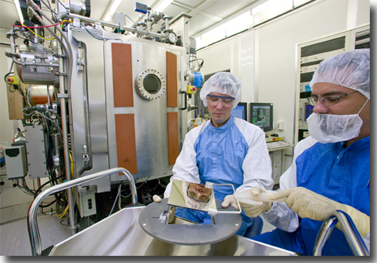
Lab materials scientist Paul Mirkarimi (left) and mechanical technician Jeff Robinson are shown loading a mask blank substrate for defect smoothing. Using the technique of defect smoothing, researchers planarize tiny particles and pits to render a nearly perfect surface for masks used in extreme ultraviolet lithography, a process developed to produce computer chips that are faster and have more memory.
Earlier this year, a new way of manufacturing computer chips, developed in large measure by researchers from LLNL and two other national laboratories, won an important endorsement.
In April, the extreme ultraviolet lithography (EUVL) technology drew support at a 2008 Technology Symposium in San Jose, as the Taiwan Semiconductor Manufacturing Co. (TSMC) Ltd. outlined its lithography roadmap for the future, according to EE Times.
A silicon foundry giant, TSMC has taken a new position on the EUVL technology and provided its backing. It has placed both EUVL and maskless lithography on its roadmap for producing 15-nanometer and perhaps 22-nanometer feature-size computer chips in the future. (Currently, semiconductor manufacturers are producing computer chips with 45-nanometer feature sizes).
Much of the research and development to advance the EUVL technology has been accomplished by scientists and engineers from LLNL, Sandia National Laboratories/California and Lawrence Berkeley National Laboratory.
In 1997, a Virtual National Laboratory — made up of researchers from the three labs — was established to develop the EUVL technology for the commercial manufacturing of computer chips.
The research, set up under a $250 million cooperative research and development agreement (CRADA), one of the largest in Department of Energy history, was funded by a consortium of semiconductor firms. Eventually, the consortium included Intel Corp., Motorola Inc., Advanced Micro Devices Inc., Micron Technology Inc., Infineon Technologies and International Business Machines.
The EUVL technology offers the potential to manufacture computer chips with dozens of times more speed and hundreds of times more memory than today’s integrated circuits.
At the height of the research venture, about 175 scientists, engineers and technicians at the three national laboratories worked on overcoming the hurdles to allow EUVL to be utilized for future integrated circuit production.
During the six principal years of the CRADA, between 1997 and 2003, LLNL scientists and engineers involved in the EUVL effort garnered or played roles in winning seven prestigious R&D 100 awards, often called the "Oscars of invention." In addition, Livermore researchers received or assisted in the development of at least 50 patents.
"The EUVL project was extremely interesting and enabled us to perform some particularly innovative research," said materials scientist Paul Mirkarimi, one of the members of the LLNL team. "In the early years, we had major resources and that was a huge help."
Since the EUVL research effort has concluded, Mirkarimi sees some uncertainty about whether the process will be deployed to produce computer chips – but he is hopeful. "I really want to see this technology make it. I am now consulting for a company that is bringing an important part of the process to the market and I want to see the EUVL technology move forward."
In the five years since the main EUVL research ended at the national labs, the semiconductor consortium has continued to fund some projects, including work at LLNL to fabricate zero defect EUVL masks.
In late 2007, the Laboratory received a letter from three Intel Components Research officials praising the "outstanding contributions" of Mirkarimi, Lab mechanical technician Jeff Robinson, Lab engineering associate Sherry Baker and Lab participating guest Eberhard Spiller.
"Specifically, we appreciate their efforts in enabling one significant approach toward the realization of defect-free EUV mask blanks, and their effective project management during 2007," the Intel officials wrote.
In the end, the LLNL researchers and engineers developed a process to planarize substrate particles and pits on the masks simultaneously to, or below, one nanometer in height.
"When we started," Mirkarimi recalls, "almost no one thought we could achieve this level."
A Woodbury, N.Y.-based firm, Veeco Instruments, has designed and built a multimillion dollar tool to perform the LLNL smoothing process on masks used in EUVL work. The machine achieves the same results as LLNL has produced. In addition, the instrument has been installed at SEMATECH’s Nanotech Center in Albany, N.Y.
One important challenge remains for the technology’s mask effort. While particles and pits can be smoothed quickly, this work still needs to be done cleaner, according to Mirkarimi.
Other key advances also are needed, Mirkarimi believes, for the source, which will produce the EUVL light that travels through the lithography system and hits the wafer, and for the resist, the polymer-based compound that enables small feature sizes to be created on the wafer.
The Livermore materials scientist sees the chances of the EUVL process someday producing computer chips at 50-50 — not bad odds for what some would consider a transformational breakthrough.


