New tools that model 3D structure of amorphous materials to transform technology driven R&D
 (Download Image)
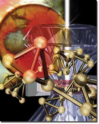
The production of amorphous red phosphorus was first reported by A. Vogel in 1813. Now pressure-dependent 3D atomic structure models have been constructed to be consistent with neutron and X-ray diffraction diamond anvil cell data. Image by Scott Dougherty/LLNL.
Click for higher resolution image
(Download Image)
The production of amorphous red phosphorus was first reported by A. Vogel in 1813. Now pressure-dependent 3D atomic structure models have been constructed to be consistent with neutron and X-ray diffraction diamond anvil cell data. Image by Scott Dougherty/LLNL.
Click for higher resolution image
LIVERMORE, Calif. — Researchers have accurately identified tools that model the atomic and void structures of a network-forming elemental material. These tools may revolutionize the process of creating new solar panels, flat-panel displays, optical storage media and myriad other technological devices.
The team, made up of researchers from Lawrence Livermore National Laboratory, Rutherford Appleton Laboratory and Lawrence Berkeley National Laboratory, created 3D models of pressure-dependent structures of amorphous red phosphorus (an allotrope of the element phosphorous with different structural modifications) that for the first time are accurately portrayed by neutron and X-ray diffraction studies. They also developed a new method to accurately characterize void structures within network-forming materials.
These results on an elemental material serve as a benchmark indicating the ability of their analysis tools to accurately portray the entire structure of multi-atomic amorphous material systems. The mechanical, optical, magnetic and electronic plasticity of amorphous materials hold great promise toward enhancing current and emergent technologies. The new tools will build more systematic design paths leading to R&D advances.
Amorphous red phosphorus (a-rP) was first reported to be formed by A. Vogel in 1813 when sunlight was focused onto white phosphorus. During the 20th century, a-rP was studied intensely using a wide array of experimental and theoretical tools.
Beginning in the 1970s and ’80s, amorphous or disordered materials were found to exhibit technologically viable properties by their central role in photovoltaic cells and portable opto-electronic storage media such as CDs, DVDs, and more recent Blu-Ray disks. However, attempts by scientists to accurately characterize seemingly simple elemental materials like a-rP were hindered because the appropriate analysis tools simply did not exist.
But the recent team of scientists: Joseph Zaug of LLNL, Alan Soper of Rutherford and Simon Clark of LBL, conducted X-ray and micro-Raman measurements of a-rP as a function of applied pressure and developed diffuse scattering analysis tools to unambiguously reveal not only 3D atomic structures, but also the void structures that significantly affect bulk material properties.
X-ray patterns of many amorphous materials reveal an unusually narrow and sometimes remarkably intense diffraction peak. The first sharp diffraction peak (FSDP) of multi-atomic systems is now predominately accepted to be associated with atomic scale voids that result from chemical-chemical bonding geometries.
As reported in the study that appears in the Oct. 12 online edition of the journal Nature Materials , the new void analysis tools may reveal that multi atomic amorphous material voids occur more simply from density-density fluctuations.
The diffuse scattering analysis tools developed by these scientists will enable more systematic engineering routes toward design and characterization of amorphous materials.
The team used the Advanced Light Source, Beam line 12.2.2, at Lawrence Berkeley Laboratory to conduct the X-ray scattering measurements.
Contact
Anne M. Stark[email protected]
925-422-9799
Related Links
"Pressure-dependent structures of amorphous red phosphorus and the origin of the first sharp diffraction peaks,"Materials Sciences Division
Checking out the hot spots
Joe Zaug
Nuclear and Chemical Science Division


