Lab wins three FLC awards for tech transfer
 (Download Image)
L3-HAPLS — the world’s most advanced and highest average power, diode-pumped petawatt laser system — was designed, developed and constructed in only three years by Lawrence Livermore National Laboratory’s NIF and Photon Science Directorate and delivered to ELI Beamlines in June 2017. Photo by Jason Laurea/LLNL
(Download Image)
L3-HAPLS — the world’s most advanced and highest average power, diode-pumped petawatt laser system — was designed, developed and constructed in only three years by Lawrence Livermore National Laboratory’s NIF and Photon Science Directorate and delivered to ELI Beamlines in June 2017. Photo by Jason Laurea/LLNL
Three teams of Lawrence Livermore National Laboratory (LLNL) scientists, each supported by a Lab business development executive, have captured regional awards for technology transfer from the Federal Laboratory Consortium (FLC).
This year’s awards, two for outstanding commercialization success and one for outstanding technology development, were presented Aug. 29 during the FLC’s three-day Far West/Mid-Continent regional meeting at the Skirvin Hilton Hotel in Oklahoma City.
Started in 1974, the FLC assists the U.S. public and private sectors in using technologies developed by federal research labs. It is comprised of more than 300 federal labs and research centers.
Since 2007, LLNL has garnered 33 regional awards for technology transfer from the FLC.
Advanced petawatt laser
One of the Lab researchers’ two awards for outstanding commercialization success featured one of Livermore’s largest-ever technology transfer projects — the design, development and construction of an advanced petawatt laser system.
Under a $52 million agreement with the Czech Republic’s European Extreme Light Infrastructure (ELI), Lab researchers developed and constructed the laser system in only three years from concept to product, delivering the laser to the facility in June 2017.
Known as the High-repetition-rate Advanced Petawatt Laser (HAPLS), the new laser system was designed and constructed by LLNL’s NIF and Photon Science Directorate (NIF&PS).
What makes HAPLS unique is its repetition rate and repeatability. It can fire up to 10 times per second and deliver in each of these pulses the peak power of 1 quadrillion watts — an order of magnitude faster than any other high-peak power laser in the world. This high repetition rate translates into photon flux that is important for commercial applications: HAPLS can deliver up to about 1.1 megajoules per hour of petawatt pulses. Furthermore, the high repetition rate allows exploration of new science with unprecedented precision.
After an evaluation by an international peer review group, the HAPLS petawatt laser was declared fully integrated and operational at the ELI Beamlines Research Center in Dolní Břežany, Czech Republic in June. The group assessed the laser performance, determined that all required performance parameters had been successfully met and that the system was ready for integration with the experimental systems as well as for first experiments.
Leading the HAPLS project allowed LLNL to draw on its decades of pioneering laser research and development and apply that expertise to advance new laser concepts important for its mission as a national laboratory. The collaboration extended beyond LLNL and ELI Beamlines. By partnering with industry — and drawing on LLNL’s expertise in laser research and development — the team provided a number of critical advances.
Constantin Haefner, the program director for Advanced Photon Technologies at LLNL, notes that in the drive to achieve the far-reaching objectives of the HAPLS project, LLNL and its industrial partners jointly developed revolutionary components that are now on the market and that led to new business opportunities.
The LLNL-Czech partnership was made possible through an Agreement for Commercializing Technology (ACT) — a new technology transfer mechanism piloted by the U.S. Department of Energy in June 2012.
This mechanism was conceived to help national laboratories form research partnerships using contractual terms better aligned with industry practice. Under an ACT, national lab contractors may take on financial risk that the U.S. government cannot assume.
In addition to Haefner, other key leaders in the technology transfer effort included Andy Bayramian, LLNL systems architect; Thomas Spinka, LLNL short pulse commissioning manager; Dan Mason, LLNL chief mechanical engineer; Jeff Horner, LLNL project manager; Craig Siders, senior scientist and commercial technology development leader; Genaro Mempin and David Dawes, business development executives from the Lab’s Innovation and Partnerships Office (IPO); Roman Hvezda, ELI project manager; and Bedřich Rus, ELI laser delivery manager.
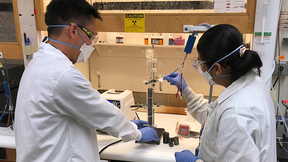
Nitrogen oxide detector
A nitrogen oxide detector for diesel engines that has been developed by LLNL scientists and is being commercialized by a Colorado-based company, CoorsTek Sensors, was named an outstanding commercialization success by the FLC.
The electrochemical solid-state detector could be an important step in the development of accurate and affordable emissions sensors for diesel engines in cars, commercial and marine vehicles, locomotives and stationary equipment.
Existing nitrogen oxide detectors are expensive and fragile, limiting their adoption, especially in applications that require low costs while adhering to emissions standards.
The Livermore/CoorsTek nitrogen oxide detector is simple and inexpensive, potentially opening the door to a $2.5 billion industry by 2023, as the regulation of diesel engines continues to expand.
"Sensors are needed that will be able to detect down to single part-per-million levels, and they must be accurate, inexpensive ($50 or less for cars), compact, usable under extremely harsh chemical and temperature regimes, and easily integrated into existing platforms," said retired LLNL chemist Robert Glass, one of the key developers of the technology.
In 2011, the LLNL-developed nitrogen oxide detection technology was licensed to a venture-backed developer of advanced sensor technologies called EmiSense. In turn, EmiSense concluded a 30-month cooperative research and development agreement (CRADA) to advance the technology.
Later, in 2014, EmiSense hired LLNL materials scientist Leta Woo, who co-developed the technology with Glass.
"EmiSense further developed the technology to be more suitable for commercialization and manufacturing," Woo said, adding that the firm’s upgrades improved the sensor’s durability, stability and capabilities.
In 2014, EmiSense was acquired by CoorsTek Sensors; they expect the technology to hit the market within the next several years.
"For technologies with significant government investment, the partnership between LLNL and EmiSense is a premium example of how national labs can and should interact with startup companies as they move toward commercialization," said Livermore IPO Business Development Executive Annemarie Meike.
"LLNL’s early stage intellectual property inspired the partnership, but the concept did not remain in its original form for long. It morphed significantly along the way as the partners shared their expertise. This is what we hope to see in a great collaboration," Meike added.
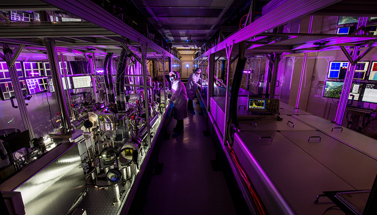
System writes tiny — and ultra-fast
Two LLNL engineers, working in collaboration with researchers from the Chinese University of Hong Kong, have developed a femtosecond projection lithography system (a femtosecond is one quadrillionth of a second).
The development of the new system, dubbed FemtoProWrite, has netted the international team an FLC outstanding technology development award.
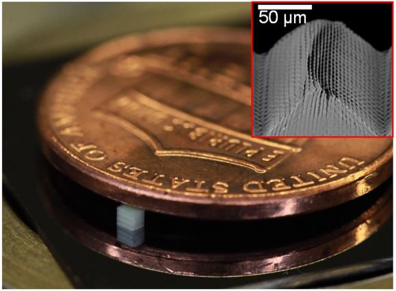
FemtoProWrite is an additive manufacturing (AM) system for the high-speed writing of complex 3D plastic structures with submicron features. AM is used to fabricate 3D structures by enabling fine control of the geometry and material properties of the different building blocks.
Submicron AM allows this level of control on a scale 100 to 1,000 times finer than a human hair.
Using the fine resolution of submicron AM, the technology has been used in a wide variety of fields to fabricate functional micro- and nanoscale 3D structures for photonic crystals, optical and mechanical metamaterials, micro fluidics, miniaturized optics and flexible electronics.
The small-scale features in these structures are key to achieving the superior functionality of low-density, high-stiffness structural materials, fast-charging solid-state batteries, efficient photovoltaics and high-sensitivity chemical and biological sensors.
It is estimated that the size of the market for products enabled by submicron AM will be between $5 to $24 billion by the year 2030. Unfortunately, the commercially available manufacturing capability for submicron AM is too slow for mass production and real-world use of these functional micro- and nanoscale structures.
FemtoProWrite increases the throughput of submicron AM by a factor of at least 35 times without degrading the submicron resolution.
To perform high-speed AM of 3D structures with submicron features, FemtoProWrite leverages two-photon polymerization (TPP). TPP is a light-directed writing technique in which chemical reactions initiated by light lead to a change in the phase of a material from liquid to solid within a region that is smaller than the light spot.
The two Livermore researchers who led the development efforts for FemtoProWrite are mechanical engineers Sourabh Saha and Vu Nguyen, who is a postdoctoral fellow.
Contact
 Stephen Wampler
[email protected]
(925) 423-3107
Related Links
Federal Lab ConsortiumTags
Economic ImpactIndustry Collaborations
Technology Transfer
Featured Articles