HPC4Manufacturing project aims at improving thin-film processes used in LED lights
 (Download Image)
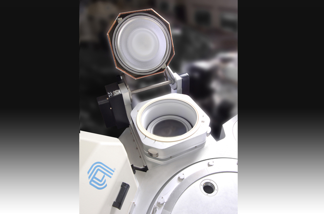
A single wafer process chamber used by Applied Materials to perform physical vapor deposition on any type of wafer, including the sapphire substrates used in the HPC4Manufacturing collaboration with Lawrence Livermore National Laboratory. Photo courtesy of Applied Materials.
(Download Image)
A single wafer process chamber used by Applied Materials to perform physical vapor deposition on any type of wafer, including the sapphire substrates used in the HPC4Manufacturing collaboration with Lawrence Livermore National Laboratory. Photo courtesy of Applied Materials.
Lawrence Livermore National Laboratory (LLNL) researchers are working with semiconductor chip manufacturer Applied Materials to improve a process for depositing thin-film materials on wafers that are used in high-efficiency LED lights and other products. The Department of Energy’s High Performance Computing for Manufacturing (HPC4Manufacturing) program is funding the effort.
Reliably creating thin films with favorable electrical, optical, structural and chemical properties is an important problem in manufacturing. One possible technique for depositing thin films with controlled properties is high-powered impulse magnetron sputtering (HiPIMS), which has yet to be optimized because modeling magnetron plasma discharges at relevant densities is a "grand challenge computing problem," researchers said.
Magnetron sputtering involves repeatedly bombarding a "target" with high-density plasma (containing ions and electrons), causing material to break from the target and "sputter" onto a substrate, such as a silicon wafer. In HiPIMS, a variant of magnetron sputtering, the plasma is typically high-energy and pulsed. The main advantage to HiPIMS, researchers said, is that they can ionize more of the sputtered material, giving them better control over uniformity and density of the resulting film.
Using LLNL’s high-performance computing systems Cab and Quartz with a commercial code called Chicago, researchers have been able to model how the plasma behaves during the HiPIMS process in three dimensions, bringing a predictive capability to the process and helping scientists determine how reactor geometry can be tailored to get the properties and uniformity that industry requires for optimal device performance.
"Essentially, having a model like this you can learn everything you want to know about the plasma," said LLNL researcher Andrea Schmidt, principal investigator on the project. "You can track things on the atomic level, where they came from, where they’re going to. These magnetron plasmas can have complex magnetic field structures. Applied Materials has a reactor they think is secret sauce — we could look into other geometries and see if we can tweak it to get what they want without trying all these configurations experimentally."
Lawrence Livermore and Applied Materials entered into a cooperative research and development agreement in summer 2017 and the project started shortly thereafter. Miller Allen, the principal investigator on the project for Applied Materials, said by using the Chicago code and LLNL’s HPC resources, the team was able to obtain a close match of the modeled voltage and current to the company’s experimental results, at realistic plasma powers, for the first time.
"The collaboration with the LLNL plasma modeling experts has been very exciting," Allen said. "Previously, we have only been able to model 3D geometries at two to three orders of magnitude below the actual operating range due to the computational complexity and computing cost of modeling dense plasmas.
Through the HPC4Mfg collaboration, we have gained immediate insights into the plasma initiation, structure and evolution that are directly applicable to our future chamber design."
Initially, the plasma models weren’t meeting expectations, Schmidt said, but eventually the modeling team, including Ihor Holod and Tony Link, got the model running reliably, first in 2D and then in 3D, using deposition rates to compare the model to experimental data.
Holod said the result is a unique capability for 3D modeling HiPIMS with realistic plasma parameters, device size and operating voltage. Dynamics and interactions of multiple particle species, including electrons, noble gas neutrals and ions, as well as sputtered material in neutral and ionized states also are considered.
"After putting all the pieces of physics and numerics together, and running a long expensive simulation, we were really excited to see the agreement with experimental measurements in terms of current evolution and sputtering efficiency," Holod said. "Kinetic simulation has provided us with the insight of plasma behavior. This allows us to see the evolution of sputtered material distribution within the magnetron chamber, leading to possible optimizations by adjusting the geometry of the device. Additionally, understanding the dynamics of magnetized plasma in the vicinity of magnetron’s target can lead to potential improvement of sputtering efficiency."
Holod said the biggest challenge of the work was identifying the proper parameters for multiple complementary processes, resulting in an integrated current to be matched with the experiment. Another challenge was choosing the numerical parameters, as the teams needed to resolve a very narrow sheath region near the surface of the cathode, where ions and electrons accelerate to energies corresponding to the operating voltage.
The research team completed the first phase of the project and was recently awarded funding from DOE’s Advanced Manufacturing Office, through the HPC4Mfg program, for a second phase. This follow-on project will look at studying a wider range of HiPIMS discharge phenomena, including 3D plasma modeling of a larger magnetron and plasma volume, longer deposition times and modeling the sputter yield of reacted compounds.
For more information on HPC4Mfg, visit the web.
Contact
 Jeremy Thomas
[email protected]
(925) 422-5539
Related Links
HPC4ManufacturingTags
HPC, Simulation, and Data ScienceComputing
Engineering
Featured Articles